
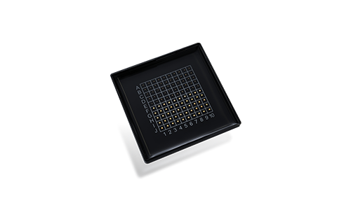
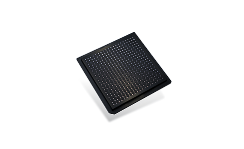
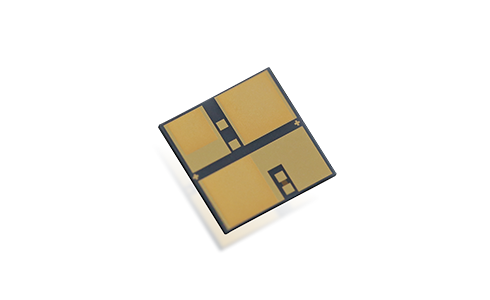
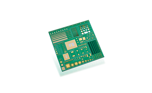
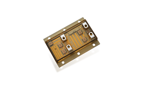















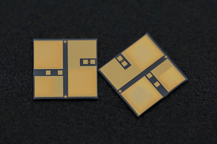
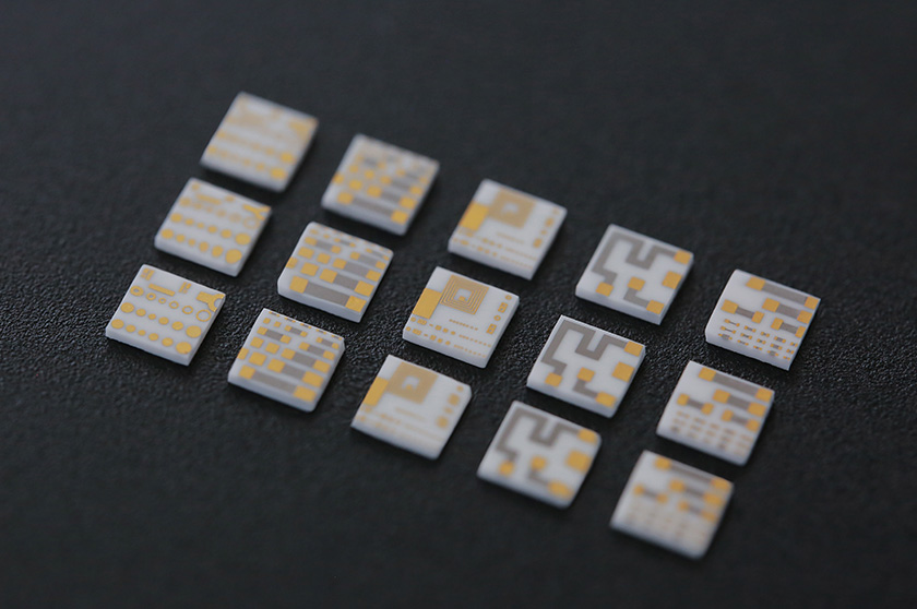
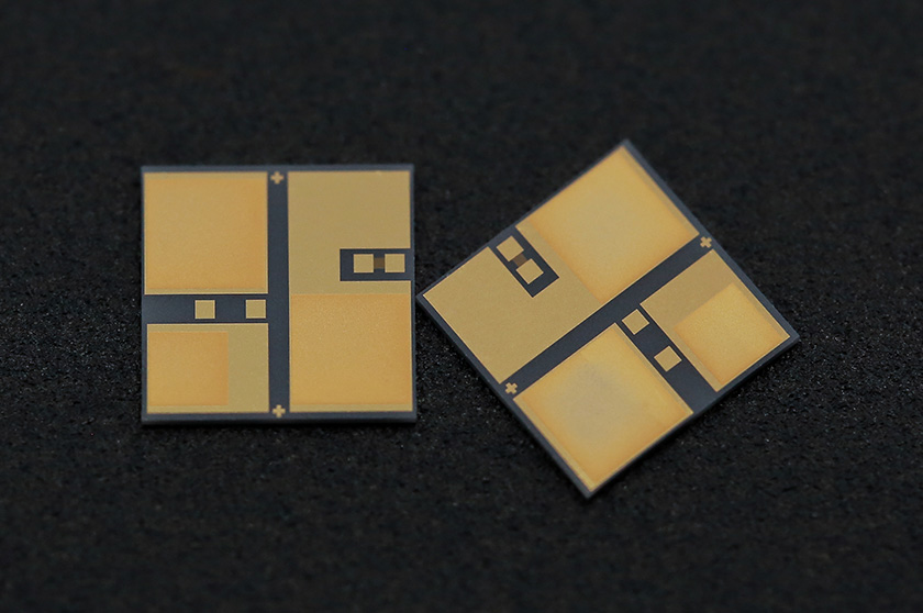
Thin Film Circuit
Size:
Custom size is available
- Sample Request
-
Download Parameters
Product Features


-
01
High reliability and stability01High reliability and stability -
02
Superior thermal conductivity02Superior thermal conductivity -
03
Excellent insulation performance with low high-frequency loss03Excellent insulation performance with low high-frequency loss
Product Applications
-
Microwave/millimeter wave devices
-
Microwave/millimeter wave circuit boards
-
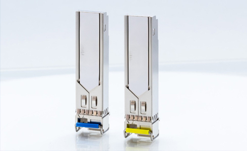
Substrates for high-speed optical communication devices
Product Selection

Swipe Left
| Substrate Materials | Material | Al2O3, AlN, Si, glass, etc. |
| Lay out | 2~6 inch. in square or round | |
| Min. size(mm) | 0.3*0.3 | |
| Tolerance(mm) | ±0.05 | |
| Thickness(mm) | 0.101~1.524 | |
| Roughness(um) | Polish<0.08, as-fired<0.8, grinding(customer specified) | |
| Metal | Sputtering materials | Ti, TiW, TaN, Cu, Ni, Pt, Au |
| Electroplating materials | Au | |
| Au thickness(um) | 0.5~5 | |
| Resistor | Material | TaN |
| Sheet resistance(Ω/SQ) | 25~200 | |
| Tolerance | ±10% | |
| Min. size(um) | 50*50 | |
| TCR(ppm/℃)(@-55~﹢125℃) | -100±50 | |
| Max. service temperature(℃)(<0.5h) | 350 | |
| Graphic | Min. line width(um) | 10 |
| Min. line gap(um) | 20 | |
| Tolerance(um) | ±3 | |
| Metallized holes/slots | Hole diameter(min.) | 0.5*T |
| Spacing between via holes(min.) | 1*T | |
| Hole to edge(min.) | 1*T | |
| Hole to metal line(min.)(um) | 38.1 | |
| Via hole to conductor edge(min.)(um) | 50.8 | |
| Tolerance(um) | ±3 | |
| Note: T is the thickness of ceramic substrate | ||